


Electron and Plasma Technologies
The Special technology department of the Institute of Scientific Instruments of the CAS in Brno deals with the development of technologies and design of technological devices, which constitute the necessary background for the construction electron-optical devices operating in a vacuum, respectively. ultra-high environment. These include primarily electron beam welding and vacuum brazing, the development and manufacture of vacuum feedthroughs, etc.
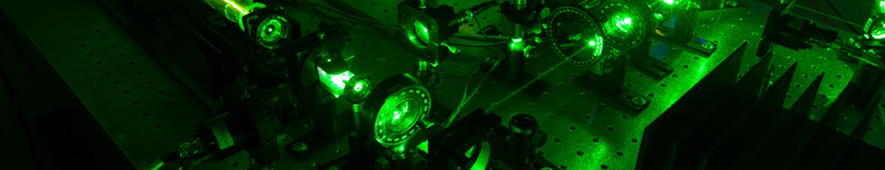
The group also deals with magnetron sputtering and the characterization of thin films. We create coatings (e.g. Al, Si, Mo, Ti, Ni, Ag, C, ITO, Nb, W, TiN Si3N4, SiO2 and their combinations). We are preparing a multi-layered system for X-ray optics with nanometer thicknesses double-layers for summary tenth micrometer thickness with an accuracy of tenths of nanometers. Cooperation with thin-layers centres in the Republic led to the examination of prospective coatings of carbon nitride, carbon, and nano-structured multi-layers and nano-composites based on carbon for the instrument. Currently, we are one of two centres in the Republic offering characterization of hard wear-resistant coatings by impact dynamic tester.
 |
|
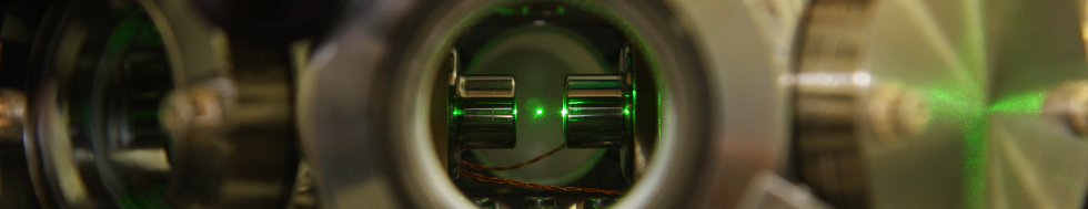
The third group of the Special technology department is the group of Electron Beam Lithography (EBL). The EBL group deals with the research and development in the field of microlithographic technologies using e-beam pattern generators. Its activity concentrates on large-size micro-structure diffractive optical elements for laser-beam forming, sub-micron diffractive holography structures for industrial holography applications, and thin-film metallic and dielectric structures on silicon substrates for sensor applications. |
