Description of the Method
Magnetron sputtering is one of the most widely used techniques for thin-film deposition. It is a physical vapour deposition (PVD) method in which material from a source (target) is transferred into the gas phase and transported towards a substrate, where it condenses to form a thin coating. During magnetron sputtering, target material is ejected by plasma. First, the deposition chamber is evacuated to a very low pressure. A process gas, typically argon, is then introduced into the chamber, where an electrical discharge is ignited by applying an electric field. During the discharge, atoms of the process gas become ionised through electron removal, creating a plasma consisting of ions and free electrons. The plasma is confined near the target by a specially configured magnetic field, which gives the method its name. Interaction between the plasma and the target surface leads to sputtering of target atoms. These particles are subsequently transported towards the substrate, where they condense and form a thin coating. Magnetron sputtering offers numerous advantages. Among the most important are excellent coating adhesion to the substrate, the possibility of low-temperature deposition, high coating quality (purity, density, and mechanical strength), and outstanding process reproducibility. Deposition parameters allow precise control of both coating thickness and chemical composition. Different plasma excitation modes enable the deposition of a wide range of materials, from metals and alloys to ceramics. By introducing reactive gases, nitrides, oxides, and carbides can be deposited, while all of these materials can also be prepared as multilayer structures.
Deposition System Parameters
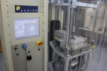
Thin coatings are prepared using two deposition systems. The Aurion magnetron sputtering system is equipped with three magnetrons, allowing deposition from three different targets with a diameter of 152 mm within a single deposition cycle. Due to high-frequency excitation, two of the targets can be electrically insulating. Deposition is performed on substrates with a maximum diameter of 90–200 mm, depending on the required coating uniformity; the maximum substrate thickness is 30 mm. The deposition system is equipped with substrate preheating and substrate biasing capabilities. Bias voltage can be used to control coating properties such as adhesion and density and can also be applied for ion etching of the substrate surface. The deposition process is fully automated, enabling the preparation of complex coating architectures, including multilayer and gradient coatings. The Aurion system is therefore used for deposition of advanced coatings and layered systems for applications in optics, X-ray optics, electronics, semiconductor technologies, and related fields. Reactive gases can be introduced to enable the deposition of nitrides, oxides, and carbides. An integrated optical emission spectrometer continuously monitors the plasma, providing feedback for process control during reactive sputtering. The second deposition system is the LEYBOLD-HERAUS Z 550. This system is also equipped with three targets, all operated using high-frequency excitation. The system provides substrate biasing and substrate preheating capabilities and can also be operated in reactive sputtering mode. It is used, for example, for deposition of DLC coatings and metallic coatings for electronic applications or electron microscopy.
Magnetron Sputtering Services
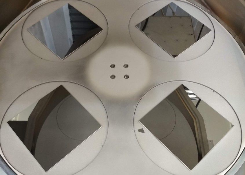
We offer thin coating deposition by magnetron sputtering for both industrial and academic clients. Our capabilities cover a wide range of thin coatings and multilayer systems. Thanks to the design of our deposition systems, we can reproducibly prepare multilayer structures with individual layer thicknesses controlled to better than one nanometre. Such coatings are particularly suitable for demanding applications, including X-ray and extreme ultraviolet (EUV) optics. The deposition system is equipped with homogenising masks, enabling highly uniform coating deposition on substrates with diameters of up to 90 mm. Drawing on many years of experience, we prepare optically and electrically functional coatings with well-defined properties, including electrical conductivity and optical reflectivity. Our portfolio includes pure metallic coatings, transparent conductive oxides (e.g. ITO and zirconium oxide-based coatings), and diamond-like carbon (DLC) coatings.
Thin coatings can be deposited on a wide range of substrates, including silicon wafers, glass, and metallic materials. Under suitable conditions, selected coating materials can be deposited at temperatures close to room temperature, making deposition on PMMA, PET, and similar polymer substrates possible. In such cases, the primary limitation is the low outgassing requirement of polymer materials under vacuum. Coatings with precisely defined properties require carefully prepared and thoroughly cleaned substrates. Where appropriate, substrate preparation and cleaning can be carried out at the Institute of Scientific Instruments prior to deposition. In addition to coating deposition, the Thin Films Group offers a broad range of coating characterisation techniques. Coating thickness is routinely measured using a Taylor Hobson contact profilometer or, for thicker coatings, by the CSM Instruments calotest method. Coatings intended for X-ray optics are characterised by X-ray diffraction in collaboration with an external partner. Additional characterisation methods include a Keyence VK-X1100 laser confocal microscope together with a range of techniques for measuring electrical conductivity, optical reflectivity, and other functional properties. Our services range from the deposition of coatings with precisely defined thickness to the development and optimisation of coatings with tailored combinations of functional properties. The scope of the services can be adapted to the specific requirements of each project. For further information about our deposition services or research collaboration opportunities, please contact us via the contact e-mail.