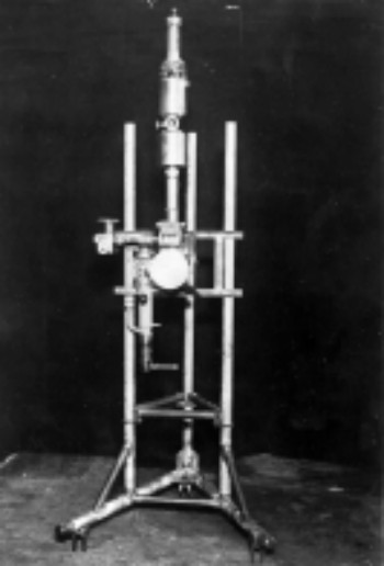
"Tripod" (1950)
The first Czechoslovak electron microscope (1950)

Further development of the first Czechoslovak electron microscope (1950)
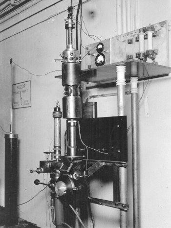
The first commercially available Czechoslovak electron microscope was developed by young electrical engineers A. Delong, V. Drahos and L. Zobac. The microscope was completed in 1951 and exhibited at the International Trade Fair in Prague. 25 of these microscopes were then produced in the science workshops of the national concern Tesla Pardubice, Brno 1 plant, under serial number Tesla BS241. The optical system of the microscope was formed of an electron gun, condenser, objective and projective lenses. The accelerating voltage was 50 kV, the resolution as little as 2 nm. The resolution was limited by the axial astigmatism of the objective, the correction of which was not a project worked on at that time.
Tesla BS241 (1951)
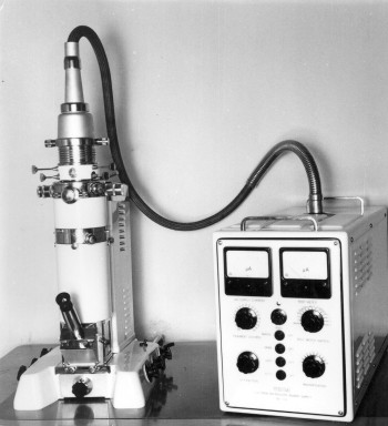
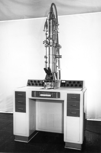
In 1950 the idea for a tabletop electron microscope was born, i.e. an instrument that would not aspire to ultimate parameters, and that would be simple, cheap and easy to operate. The instrument was completed in the Electron Optics Laboratory of the Czechoslovak Academy of Sciences, where six employees worked under the leadership of A. Delong. A number of these microscopes were produced in the developmental workshops of the CSAS, and serial production began in 1956 at Tesla Brno under serial number Tesla BS242. The instrument won a Gold Medal at the Expo 58 World Exhibition in Brussels. Tesla produced more than 1,000 of these microscopes over the following 20 years. The resolution of this microscope, already with astigmatism correction, was 5 nm, and with careful operation as little as 2 nm. The accelerating voltage was from 30 to 75 kV.
The Tesla BS242 tabletop electron microscope (1954)

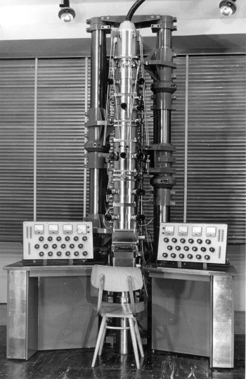
An experimental microscope with five magnetic lenses (two condensers and three imaging lenses) was put into operation in 1959. It worked with an accelerating voltage of up to 100 kV. The instrument was constructed by (from the left) L. Zobac, V. Drahos, J. Specialny and (seated) A. Delong.
Experimental transmission electron microscope - 100 kV (1960)
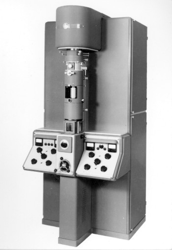
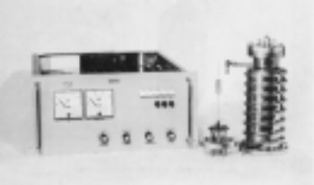
In 1962 and 1963 transmission electron microscopes allowing a resolution of down to 0.6 nm were presented to the biology institutes in Prague. Tesla in Brno began making this microscope in 1964 under serial number Tesla BS 413. This microscope was progressively adapted by the staff of the Tesla Brno development department, resulting in the modified instruments Tesla BS 513 (enabling tilting of the specimen - 1967) and Tesla BS 613 (the mechanical alignment shift and tilting of the optical system were replaced with an electromagnetic system - 1970). An adapter for the electron microscope enabling the diffraction of fast electrons was introduced in 1962. 395 of these microscopes were produced up until the end of 1975.
Tesla BS413 (1962)
Previous work in the area of wave electron optics led to an attempt to construct an electron microscope with very high resolution. This microscope was put into operation in 1968. Its accelerating voltage was 150 kV. It did not prove possible to achieve the theoretically possible resolution (0.2 nm), principally due to the inadequate mechanical stability of the instrument, though extremely valuable experience was obtained.
Experimental transmission electron microscope - 150 kV (1968)


Work was also done during the fifties and sixties on unconventional techniques in electron microscopy, such as interference electron microscopy (1963-1973), shadow electron microscopy (1965-1969), Lorentz electron microscopy (1966-1974) and diffraction under low angles (1966-1971).
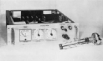
An adapter with an electrostatic biprism for a transmission electron microscope, enabling the interference electron microscopy (1963), and a diffraction pattern obtained on this biprism

The first experimental emission electron microscope, enabling mirror and tunnel microscopy, was built in 1961-1964. An ultrahigh vacuum (10-6 Pa) was achieved in the preparation chamber of the innovated instrument (1964-1967), which significantly reduced contamination of the specimen. A combined emission electron microscope was developed during the period 1970-1974, which enabled the diffraction of slow electrons and Auger spectroscopy. A large number of analysers were tested during development. Although this microscope was never produced on a commercial basis, a large number of extremely valuable results were published (see, for example, A. Delong, V. Drahos: Low energy electron diffraction in an emission microscope. Nature Phys. Sci. 230 (1971) 196-197).
Emission electron microscope (1968)

It proved necessary to develop new types of vacuum pumps for the pumping of electron optical equipments, and later to obtain an ultrahigh vacuum. The electrostatic ion gettering pump allowed extremely low pressures to be obtained, while causing no disturbance by mechanical vibrations or a magnetic field, as is the case with traditional ion gettering pumps.
The Orbitron-type ion gettering pump (1962-1963)
Titanium gettering pump (1963)
Cryosorption vacuum pump with a molecular sieve (1963)

A multipurpose vacuum furnace was built in 1965, which was suitable for various technological works, such as melting metals, the deposition of thin layers, the production of sintered feedthroughs from covar glass, capillary brazing and welding.
Multipurpose vacuum furnace (1965)

The electron beam welder allowed the welding of ultrahigh vacuum parts of microscopes developed at the Institute of Scientific Instruments. According to documents from the ISI the welder was built by a number of institutions.
Electron beam welder ES-2 (1969)

Original methods, based on the use of a resistance network, were developed at the ISI for the design of a magnetically saturated objective for a transmission microscope. These methods were later replaced by numerical calculations using the finite element method. In this way we can model both magnetic lenses and electrostatic lenses and deflectors, and determine the electron optical properties in the computed fields extremely accurately.
The use of the finite element method for the calculation of the field of electrostatic and magnetic rotationally symmetrical lenses (1974)

The conception for a scanning electron microscope with a field-emission gun came about in 1974. The gun had a cathode made from a wolfram single-crystal orientation (310) operated at room temperature, with a pressure better than 10-8 Pa in the gun area and better than 10-6 Pa in the preparation chamber. The preparation chamber was equipped with an ion gun for surface cleaning, analysers of Auger electrons and characteristic X-ray radiation and detectors of secondary, reflected, absorbed and transmitted electrons. Tesla Brno made 56 of these instruments up to 1989.
The BS 350 scanning electron microscope (1976)


It was not possible to use plastic scintillators for the detection of electrons in an ultrahigh vacuum microscope, for which reason a single-crystal scintillator based on an yttrium-aluminium garnet (YAG) began to be used - a world first in electron microscopes. The scintillator is attached to the light guide and photomultiplier situated outside the microscope.
Single-crystal scintillator based on an yttrium-aluminium garnet (YAG) for detecting electrons in electron microscopes (1978)
The heads of detectors of backscattered electrons for high-resolution electron microscopy (1983)

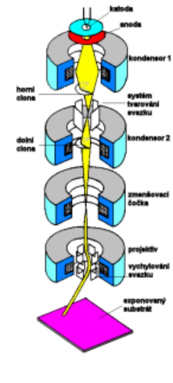
The electron beam lithograph contained a number of original solutions: a Schottky gun with high brightness, precise beam deflection, laser controlled motions of the specimen stage, and fast-response electronics.
Electron beam lithograph (1985)
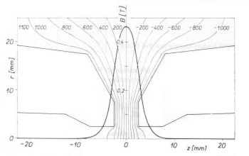
The principle of the optical system of the electron beam lithograph allowing a unique method of shaping the orthogonal cross-section of the electron beam, i.e. the "stamp", placed at any point in the exposure field of the lithograph.
The basic principle of the optical system of the electron beam lithograph (1985)
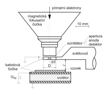
A special diagnostic microscope, working with a field-emission source of electrons with a primary electron energy range from 300 eV to 5 keV was designed for testing integrated circuits. The instrument was fitted with an energy analyser of secondary electrons and rapid beam-blanking system, allowing accurate measurements of the potential at any given point of the integrated circuit and mapping the waveform of a high-frequency signal.
Diagnostic electron microscope (1988)
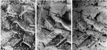
The scanning electron microscope was fitted with a cathode lens enabling high-resolution imaging throughout the entire energy range of incident electrons, generally from 1 eV to 10 keV. The first series of images of this type, impossible with a scanning electron microscope until that time, were presented at a conference in 1990. The photograph shows an image of polycrystalline copper in a Tesla BS 340 microscope at energies of 5 keV (left), 200 eV (middle) and 10 eV (right).
Adaptation of a commercial scanning electron microscope to microscopy with very slow electrons (1993)

The first environmental scanning electron microscope in the Czech Republic for observing samples in their natural state (1996)